找回密码
 To register

QQ登录

只需一步,快速开始

扫一扫,访问微社区

Titlebook: Scanning Probe Microscopy; Electrical and Elect Sergei Kalinin,Alexei Gruverman Book 2007 Springer-Verlag New York 2007 AFM.KLTcatalog.Micr

[复制链接]
查看: 51146|回复: 54
发表于 2025-3-21 16:44:19 | 显示全部楼层 |阅读模式
书目名称Scanning Probe Microscopy
副标题Electrical and Elect
编辑Sergei Kalinin,Alexei Gruverman
视频video
概述Appeals to researchers from disciplines as diverse as physics, chemistry, biology, molecular engineering and biotechnology.Presents practical aspects of materials characterization as applied to semico
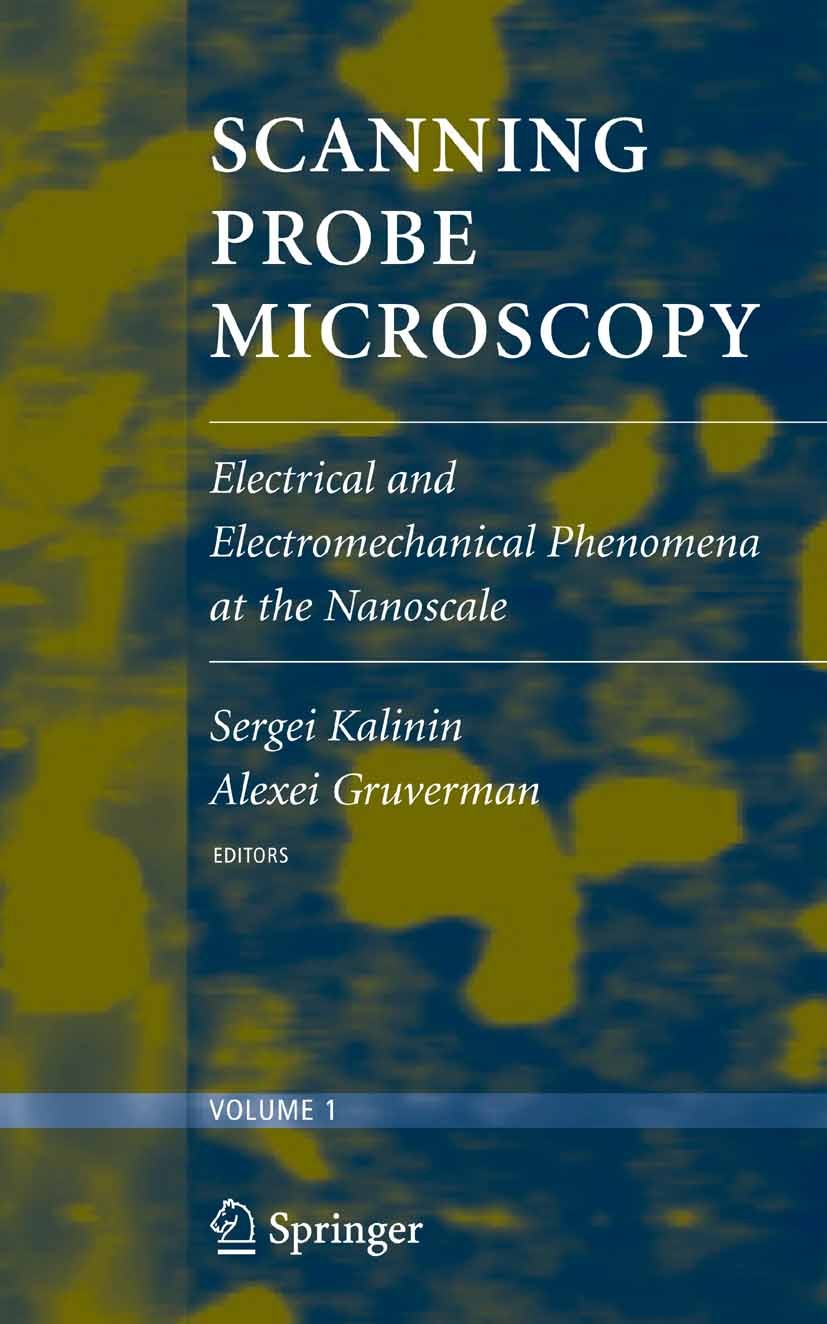
图书封面Titlebook: Scanning Probe Microscopy; Electrical and Elect Sergei Kalinin,Alexei Gruverman Book 2007 Springer-Verlag New York 2007 AFM.KLTcatalog.Micr
描述.Scanning Probe Microscopy brings up to date a constantly growing knowledge base of electrical and electromechanical characterization at the nanoscale. This comprehensive, two-volume set presents practical and theoretical issues of advanced scanning probe microscopy (SPM) techniques ranging from fundamental physical studies to device characterization, failure analysis, and nanofabrication. Volume 1 focuses on the technical aspects of SPM methods ranging from scanning tunneling potentiometry to electrochemical SPM, and addresses the fundamental physical phenomena underlying the SPM imaging mechanism. Volume 2 concentrates on the practical aspects of SPM characterization of a wide range of materials, including semiconductors, ferroelectrics, dielectrics, polymers, carbon nanotubes, and biomolecules, as well as on SPM-based approaches to nanofabrication and nanolithography. .
出版日期Book 2007
关键词AFM; KLTcatalog; Microscopy; Nanotube; PED; Polymer; REM; STEM; STM; carbon nanotubes; electronics; mechanics; p
版次1
doihttps://doi.org/10.1007/978-0-387-28668-6
isbn_softcover978-1-4939-5036-2
isbn_ebook978-0-387-28668-6
copyrightSpringer-Verlag New York 2007
The information of publication is updating

书目名称Scanning Probe Microscopy影响因子(影响力)


书目名称Scanning Probe Microscopy影响因子(影响力)学科排名


书目名称Scanning Probe Microscopy网络公开度


书目名称Scanning Probe Microscopy网络公开度学科排名


书目名称Scanning Probe Microscopy被引频次


书目名称Scanning Probe Microscopy被引频次学科排名


书目名称Scanning Probe Microscopy年度引用


书目名称Scanning Probe Microscopy年度引用学科排名


书目名称Scanning Probe Microscopy读者反馈


书目名称Scanning Probe Microscopy读者反馈学科排名


单选投票, 共有 1 人参与投票
 

0票 0.00%

Perfect with Aesthetics


0票 0.00%

Better Implies Difficulty


1票 100.00%

Good and Satisfactory


0票 0.00%

Adverse Performance


0票 0.00%

Disdainful Garbage

您所在的用户组没有投票权限
发表于 2025-3-21 21:47:41 | 显示全部楼层
Scanning Probe Microscopy on Low-Dimensional Electron Systems in III–V Semiconductorsed the effort to observe the local arrangement of the electrons in real space by scanning probe techniques. In this chapter the current state of the art of the different scanning probe methods as applied to low-dimensional III-V semiconductors is reviewed and the specific advantages and drawbacks are discussed.
发表于 2025-3-22 01:50:11 | 显示全部楼层
发表于 2025-3-22 07:21:03 | 显示全部楼层
发表于 2025-3-22 09:58:42 | 显示全部楼层
Review of Ferroelectric Domain Imaging by Piezoresponse Force Microscopyf polarization reversal at the nanoscale, domain dynamics, degradation effects, and size-dependent phenomena in ferroelectrics are reviewed in detail. Examples of using PFM for the characterization of various polar materials such as ferroelectric films, piezoelectric semiconductors, and ferroelectric relaxors are given.
发表于 2025-3-22 13:36:13 | 显示全部楼层
Electromagnetic Singularities and Resonances in Near-Field Optical Probesering, fluorescence, etc.), the detection of the light is achieved in the far-field regime where the . acts as a mediator between the optical near-field and the detector. Figure 1 is a schematic illustration of the SNOM principle.
发表于 2025-3-22 19:11:44 | 显示全部楼层
Introduction devices at the micro-, nano-, and atomic scale levels. While structural information can be obtained by such established techniques as scanning and transmission electron microscopy, high-resolution examination of local electronic structure, electric potential and chemical functionality is a much mor
发表于 2025-3-23 00:55:47 | 显示全部楼层
Scanning Tunneling Potentiometry: The Power of STM applied to Electrical Transportand electronic structure of materials on an atomic scale and essentially ushered in the modern field of nanoscience. The goal of scanning tunneling potentiometry (STP) is to adapt the scanning tunneling probe to measure electrical transport on the same length scale. The approach is to establish a cu
发表于 2025-3-23 03:40:35 | 显示全部楼层
Probing Semiconductor Technology and Devices with Scanning Spreading Resistance Microscopyvation of the dopants in two dimensions. For Si technology, Duane had already determined in 1996 that, in the 0.25-μm CMOS technology, a 10-nm decrease in the channel length was responsible for a more than 10% increase in the gate-to-drain overlap capacitance [.]. In the 65-nm devices processed toda
发表于 2025-3-23 06:58:29 | 显示全部楼层
Scanning Capacitance Microscopy for Electrical Characterization of Semiconductors and Dielectricso measure the capacitance between a conducting tip and sample. When applied to a semiconductor sample, an ac voltage at around 10 kHz is used to induce a depletion region within the semiconductor. The resulting differential capacitance is measured with a lock-in amplifier. The SCM contrast is propor
 关于派博传思  派博传思旗下网站  友情链接
派博传思介绍 公司地理位置 论文服务流程 影响因子官网 SITEMAP 大讲堂 北京大学 Oxford Uni. Harvard Uni.
发展历史沿革 期刊点评 投稿经验总结 SCIENCEGARD IMPACTFACTOR 派博系数 清华大学 Yale Uni. Stanford Uni.
|Archiver|手机版|小黑屋| 派博传思国际 ( 京公网安备110108008328) GMT+8, 2025-5-19 09:42
Copyright © 2001-2015 派博传思   京公网安备110108008328 版权所有 All rights reserved
快速回复 返回顶部 返回列表