| 书目名称 | Nanoscaled Semiconductor-on-Insulator Structures and Devices |
| 编辑 | Steve Hall,Alexei N. Nazarov,Vladimir S. Lysenko |
| 视频video | http://file.papertrans.cn/661/660962/660962.mp4 |
| 概述 | Reviews by leading experts in SOI nanoscaled electronics.Analysis of prospects of SOI nanoelectronics beyond Moore’s law.Explanation of fundamental limits for CMOS, SOICMOS and single electron technol |
| 丛书名称 | NATO Science for Peace and Security Series B: Physics and Biophysics |
| 图书封面 |  |
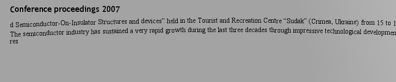
| 描述 | This proceedings volume constitutes an archive of the contributions of the key-speakers who attended the NATO Advanced Research Workshop on “Nanoscaled Semiconductor-On-Insulator Structures and devices” held in the Tourist and Recreation Centre “Sudak” (Crimea, Ukraine) from 15 to 19 October 2006. The semiconductor industry has sustained a very rapid growth during the last three decades through impressive technological developments which have resulted in products with higher performance and lower cost per function. After many years of development it is now confidently predicted that semiconductor-on-insulator materials will enter and increasingly be used by manufacturing industry. The wider use of semiconductor (es- cially silicon) on insulator materials will not only enable the benefits of these materials to be demonstrated but, also, will drive down the cost of substrates which, in turn, will stimulate the development of other novel devices and applications. Thus the semiconductor-on-insulator materials of today are not only the basis for modern microelectronics but also for future nanoscale devices and ICs. In itself this trend will encourage the promotion of the skills and idea |
| 出版日期 | Conference proceedings 2007 |
| 关键词 | Anode; CMOS; FinFET; IC; MOSFET; Nanotube; Potential; Transistor; electronics; heterojunction bipolar transis |
| 版次 | 1 |
| doi | https://doi.org/10.1007/978-1-4020-6380-0 |
| isbn_softcover | 978-1-4020-6379-4 |
| isbn_ebook | 978-1-4020-6380-0Series ISSN 1874-6500 Series E-ISSN 1874-6535 |
| issn_series | 1874-6500 |
| copyright | Springer Science+Business Media B.V. 2007 |
 |Archiver|手机版|小黑屋|
派博传思国际
( 京公网安备110108008328)
GMT+8, 2026-2-8 07:57
|Archiver|手机版|小黑屋|
派博传思国际
( 京公网安备110108008328)
GMT+8, 2026-2-8 07:57


 发表于 2025-3-21 16:41:35