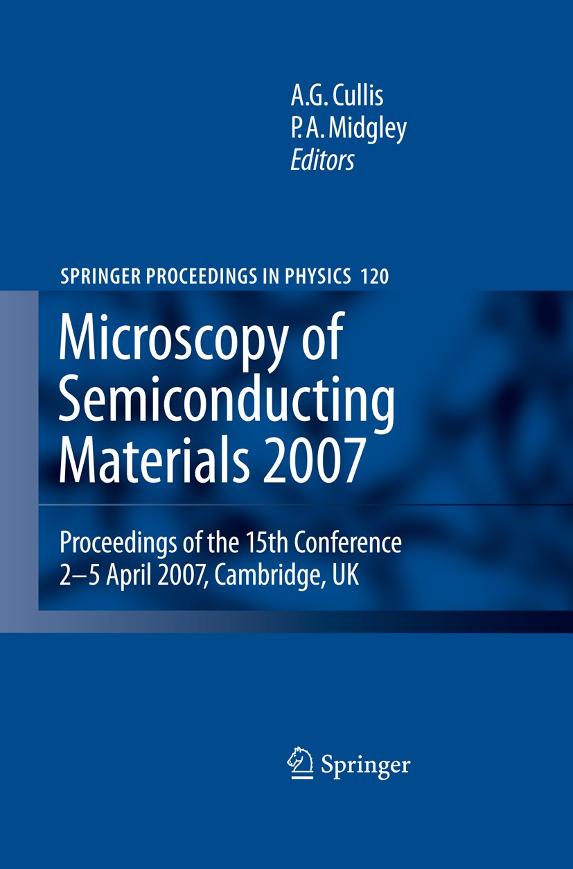
| 书目名称 | Microscopy of Semiconducting Materials 2007 |
| 副标题 | Proceedings of the 1 |
| 编辑 | A. G. Cullis,P. A. Midgley |
| 视频video | http://file.papertrans.cn/634/633445/633445.mp4 |
| 概述 | Gives a complete overview of nanostructures of all types, from quantum dots, wires to nanotubes.Complete study of the effects of semiconductor processing treatment such as oxidatorion, nitridation, io |
| 图书封面 |  |
| 描述 | This volume contains invited and contributed papers presented at the conference on ‘Microscopy of Semiconducting Materials’ held at the University of Cambridge on 2-5 April 2007. The event was organised under the auspices of the Electron Microscopy and Analysis Group of the Institute of Physics, the Royal Microscopical Society and the Materials Research Society. This international conference was the fifteenth in the series that focuses on the most recent world-wide advances in semiconductor studies carried out by all forms of microscopy and it attracted delegates from more than 20 countries. With the relentless evolution of advanced electronic devices into ever smaller nanoscale structures, the problem relating to the means by which device features can be visualised on this scale becomes more acute. This applies not only to the imaging of the general form of layers that may be present but also to the determination of composition and doping variations that are employed. In view of this scenario, the vital importance of transmission and scanning electron microscopy, together with X-ray and scanning probe approaches can immediately be seen. The conference featured developments in high |
| 出版日期 | Conference proceedings 20081st edition |
| 关键词 | Canopus; Semiconductor; Transmission electron microscopy; crystals and superlattices; electron microscop |
| 版次 | 1 |
| doi | https://doi.org/10.1007/978-1-4020-8615-1 |
| isbn_ebook | 978-1-4020-8615-1 |
| copyright | Springer Science+Business Media B.V. 2008 |
 |Archiver|手机版|小黑屋|
派博传思国际
( 京公网安备110108008328)
GMT+8, 2026-1-12 16:11


