找回密码
 To register

QQ登录

只需一步,快速开始

扫一扫,访问微社区

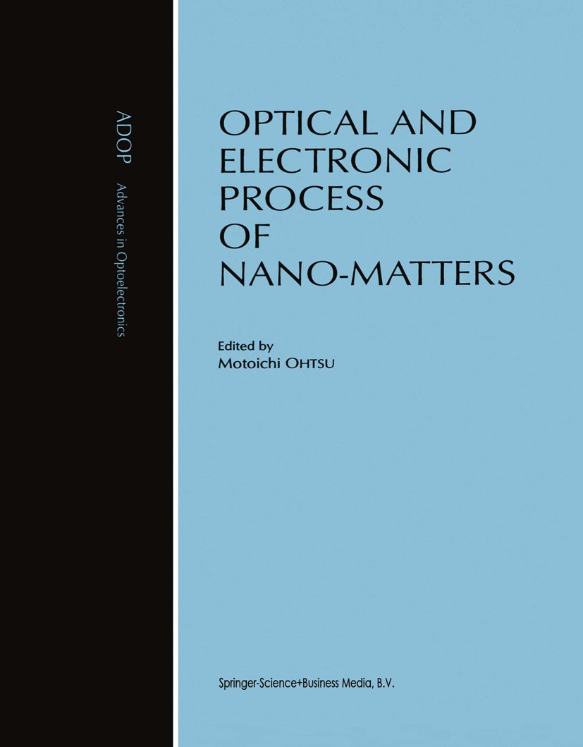
Titlebook: Optical and Electronic Process of Nano-Matters; Motoichi Ohtsu Book 2001 Springer Science+Business Media Dordrecht 2001 Evanescent wave.Op

[复制链接]
查看: 42420|回复: 50
发表于 2025-3-21 16:23:33 | 显示全部楼层 |阅读模式
书目名称Optical and Electronic Process of Nano-Matters
编辑Motoichi Ohtsu
视频video
丛书名称Advances in Opto-Electronics
图书封面Titlebook: Optical and Electronic Process of Nano-Matters;  Motoichi Ohtsu Book 2001 Springer Science+Business Media Dordrecht 2001 Evanescent wave.Op
描述Sizes of electronic and photonic devices are decreasing drastically in order to increase the degree of integration for large-capacity and ultrahigh­ speed signal transmission and information processing. This miniaturization must be rapidly progressed from now onward. For this progress, the sizes of materials for composing these devices will be also decreased to several nanometers. If such a nanometer-sized material is combined with the photons and/or some other fields, it can exhibit specific characters, which are considerably different from those ofbulky macroscopic systems. This combined system has been called as a mesoscopic system. The first purpose of this book is to study the physics of the mesoscopic system. For this study, it is essential to diagnose the characteristics of miniaturized devices and materials with the spatial resolution as high as several nanometers or even higher. Therefore, novel methods, e.g., scanning probe microscopy, should be developed for such the high-resolution diagnostics. The second purpose of this book is to explore the possibility of developing new methods for these diagnostics by utilizing local interaction between materials and electron, photo
出版日期Book 2001
关键词Evanescent wave; Optics; STEM; microscopy; quantum dot; semiconductor; spectroscopy
版次1
doihttps://doi.org/10.1007/978-94-017-2482-1
isbn_softcover978-90-481-5707-5
isbn_ebook978-94-017-2482-1
copyrightSpringer Science+Business Media Dordrecht 2001
The information of publication is updating

书目名称Optical and Electronic Process of Nano-Matters影响因子(影响力)


书目名称Optical and Electronic Process of Nano-Matters影响因子(影响力)学科排名


书目名称Optical and Electronic Process of Nano-Matters网络公开度


书目名称Optical and Electronic Process of Nano-Matters网络公开度学科排名


书目名称Optical and Electronic Process of Nano-Matters被引频次


书目名称Optical and Electronic Process of Nano-Matters被引频次学科排名


书目名称Optical and Electronic Process of Nano-Matters年度引用


书目名称Optical and Electronic Process of Nano-Matters年度引用学科排名


书目名称Optical and Electronic Process of Nano-Matters读者反馈


书目名称Optical and Electronic Process of Nano-Matters读者反馈学科排名


单选投票, 共有 1 人参与投票
 

1票 100.00%

Perfect with Aesthetics


0票 0.00%

Better Implies Difficulty


0票 0.00%

Good and Satisfactory


0票 0.00%

Adverse Performance


0票 0.00%

Disdainful Garbage

您所在的用户组没有投票权限
发表于 2025-3-21 23:25:19 | 显示全部楼层
Electron Transport in Semiconductor Quantum Dots,ble to the de Broglie wavelength of electrons. Transport measurements on these nanostructures have revealed a rich variety of phenomena associated with the effects of quantum mechanical confinement [1]. Conductance quantization in one-dimensional quantum point contacts, and resonant tunneling throug
发表于 2025-3-22 02:52:11 | 显示全部楼层
Electron Energy Modulation with Optical Evanescent Waves,to ultraviolet rays. Many kinds of electron beam devices, including the klystron, traveling wave tube (TWT), and backward wave oscillator (BWO), have been developed [1]. These beam devices have several advantages over semiconductor devices, such as a wide frequency tuning range and higher output pow
发表于 2025-3-22 08:05:57 | 显示全部楼层
发表于 2025-3-22 11:42:09 | 显示全部楼层
Theory of Electronic and Atomic Processes in Scanning Probe Microscopy,ls science, i.e., the science of nano-scale materials has been brought about thanks to the development of SPM. In spite of the rapid development in SPM as an experimental tool, however, a firm theoretical basis for it has not in general been fully established. It is only for the fundamental aspects
发表于 2025-3-22 14:37:01 | 显示全部楼层
Tunneling-Electron Luminescence Microscopy for Multifunctional and Real-Space Characterization of Snd these properties are very different from those in macroscopic structures. [1] Progress in crystal growth and micro-process technology has enabled the atomically controlled fabrication of artificial semiconductor nanostructures and devices. These have been actively studied for the purpose of achie
发表于 2025-3-22 18:38:03 | 显示全部楼层
Near-Field Optical Spectroscopy of Single Quantum Dots, highly localized features and their distributions well beyond the diffraction limit of light [1–7]. The heart of NSOM is a near-field probe, illustrated in Fig. 7.1 which is a metal-coated optical fiber tapered to an opening (aperture) which is much smaller than the wavelength of light. When the pr
发表于 2025-3-22 23:07:48 | 显示全部楼层
发表于 2025-3-23 04:26:09 | 显示全部楼层
Noncontact Atomic Force Microscopy,face images of both conductors and insulators. For several layered and nonlayered materials [2–5], atomic resolution has been achieved in the contact mode. However, the question has been raised as to whether the AFM operating in the contact mode is really a microscope like the scanning tunneling mic
发表于 2025-3-23 07:07:05 | 显示全部楼层
Correlation between Interface States and Structures Deduced from Atomic-Scale Surface Roughness in eliability of ultrathin gate oxides. [2] Because the thickness of the structural transition layer is in the order of 1 nm [3,4] and the amount of electronic defect states in the structural transition layer must be larger than that in bulk SiO., the reliability of gate oxides must be mainly determine
 关于派博传思  派博传思旗下网站  友情链接
派博传思介绍 公司地理位置 论文服务流程 影响因子官网 SITEMAP 大讲堂 北京大学 Oxford Uni. Harvard Uni.
发展历史沿革 期刊点评 投稿经验总结 SCIENCEGARD IMPACTFACTOR 派博系数 清华大学 Yale Uni. Stanford Uni.
|Archiver|手机版|小黑屋| 派博传思国际 ( 京公网安备110108008328) GMT+8, 2025-5-26 10:17
Copyright © 2001-2015 派博传思   京公网安备110108008328 版权所有 All rights reserved
快速回复 返回顶部 返回列表