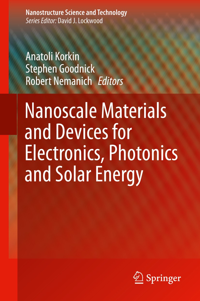
| 书目名称 | Nanoscale Materials and Devices for Electronics, Photonics and Solar Energy | | 编辑 | Anatoli Korkin,Stephen Goodnick,Robert Nemanich | | 视频video | http://file.papertrans.cn/661/660939/660939.mp4 | | 概述 | Provides an authoritative overview of the current status and future trends of nanoelectronics, photonics, and solar energy.Presents broad-ranging tutorials on both theoretical and experimental aspects | | 丛书名称 | Nanostructure Science and Technology | | 图书封面 |  | | 描述 | .This book presents research dedicated to solving scientific and technological problems in many areas of electronics, photonics and renewable energy. Progress in information and renewable energy technologies requires miniaturization of devices and reduction of costs, energy and material consumption. The latest generation of electronic devices is now approaching nanometer scale dimensions; new materials are being introduced into electronics manufacturing at an unprecedented rate; and alternative technologies to mainstream CMOS are evolving. The low cost of natural energy sources have created economic barriers to the development of alternative and more efficient solar energy systems, fuel cells and batteries..Nanotechnology is widely accepted as a source of potential solutions in securing future progress for information and energy technologies. .Nanoscale Materials and Devices for Electronics, Photonics and Solar Energy. features chapters that cover the following areas: atomic scale materials design, bio- and molecular electronics, high frequency electronics, fabrication of nanodevices, magnetic materials and spintronics, materials and processes for integrated and subwave optoelectro | | 出版日期 | Book 2015 | | 关键词 | chemistry and electronics at the nanoscale; compound semiconductor nano-heterostructures; graphene bas | | 版次 | 1 | | doi | https://doi.org/10.1007/978-3-319-18633-7 | | isbn_softcover | 978-3-319-37118-4 | | isbn_ebook | 978-3-319-18633-7Series ISSN 1571-5744 Series E-ISSN 2197-7976 | | issn_series | 1571-5744 | | copyright | Springer International Publishing Switzerland 2015 |
The information of publication is updating

书目名称Nanoscale Materials and Devices for Electronics, Photonics and Solar Energy影响因子(影响力)

书目名称Nanoscale Materials and Devices for Electronics, Photonics and Solar Energy影响因子(影响力)学科排名

书目名称Nanoscale Materials and Devices for Electronics, Photonics and Solar Energy网络公开度

书目名称Nanoscale Materials and Devices for Electronics, Photonics and Solar Energy网络公开度学科排名

书目名称Nanoscale Materials and Devices for Electronics, Photonics and Solar Energy被引频次

书目名称Nanoscale Materials and Devices for Electronics, Photonics and Solar Energy被引频次学科排名

书目名称Nanoscale Materials and Devices for Electronics, Photonics and Solar Energy年度引用

书目名称Nanoscale Materials and Devices for Electronics, Photonics and Solar Energy年度引用学科排名

书目名称Nanoscale Materials and Devices for Electronics, Photonics and Solar Energy读者反馈

书目名称Nanoscale Materials and Devices for Electronics, Photonics and Solar Energy读者反馈学科排名

|
|
|
 |Archiver|手机版|小黑屋|
派博传思国际
( 京公网安备110108008328)
GMT+8, 2025-12-28 14:25


